Product Documentation
Abstract
This document contains a table entitled IBM Netfinity 7000 - System board diagrams
Content
The IBM Netfinity 7000 is comprised of several different system boards and a SCSI backplane:
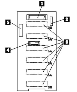
SCSI backplane component locations
The following illustration identifies the SCSI backplane components. Refer to this figure when you set the jumpers on the backplane.
Move the mouse over the index number in the illustration below. Click the index number to locate the description.
| Index | Description |
|---|---|
| 1 | Wide (16-bit) SCSI connector |
| 2 | Option jumper block (J10) |
| 3 | SCSI hot-swap drive connectors (on reverse side of backplane) |
| 4 | Repeater card connector |
| 5 | Power connector |
SCSI backplane option jumpers
The SCSI backplane option jumper block (J10) defines the SCSI IDs for hot-swap drives.
| Pins | Description |
|---|---|
| 1-2 | Reserved. |
| 3-4 | Reserved. |
| 5-6 | Placing a jumper on these two pins enables SCSI IDs 8-13 |
| 7-8 | Reserved. |
| 9-10 | Reserved. |
| 11-12 | Placing a jumper on these two pins reverses the SCSI IDs on the backplane |
NOTE: The default is no jumpers installed on the J10 jumper block.
SCSI IDs for hot-swap hard disk drives| J10 pins 5-6 | J10 pins 11-12 | Bay 1 | Bay 2 | Bay 3 | Bay 4 | Bay 5 | Bay 6 |
|---|---|---|---|---|---|---|---|
| No jumper (1) | No jumper (1) | 0 | 1 | 2 | 3 | 4 | 5 |
| No jumper | Jumper | 5 | 4 | 3 | 2 | 1 | 0 |
| Jumper | No jumper | 13 | 12 | 11 | 10 | 9 | 8 |
| Jumper (2) | Jumper (2) | . | . | . | . | . | . |
NOTES:
- This is the default jumper setting.
- This combination is not supported.
System board component locations
The following illustration identifies the system board components.
Move the mouse over the index number in the illustration below. Click the index number to locate the description.
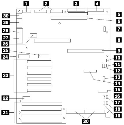
NOTE: The SCSI-A controller is connected to hot-swap bank B; the SCSI-B controller is connected to hot-swap bank A.
Memory board component locations
The following illustration identifies the memory board components.
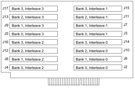
NOTES:
- The server uses 60 ns, 168-pin, error correction code (ECC), dual inline memory modules (DIMMs).
- The memory board contains four banks (0–3), arranged in 16 DIMM connectors and supports 4-way memory interleaving.
- You can install a maximum of 4 GB of memory in the server, with 256 MB memory modules in all 16 connectors (J2 through J17).
- Each bank contains connectors for four memory modules. The memory module kit sizes available for the server are 64 MB, 128 MB, and 256 MB. As a minimum, the server requires 1 full bank of memory.
- To ensure proper server operation, you must maintain 4, 8, 12, or 16 memory modules in the server. All the DIMMs installed in a bank must be the same size, but different banks can have different sized DIMMs
Memory configuration examples
The base memory is four 64 MB DIMMs. The DIMMs are installed in bank 0, connectors J2-J5.
You want four 64 MB DIMMS, eight 128 MB DIMMs and four 256 MB DIMMs in the server. Leave the 64MB DIMMS in bank 0, connectors J2-J5 and install the 128 MB DIMMS in bank 1, connectors J6-J9 and bank 2 connectors J10-J13 and the 256 MB DIMMs in bank 3, connectors J14-J17.
Additional information
Document Location
Worldwide
Was this topic helpful?
Document Information
Modified date:
24 January 2019
UID
ibm1MIGR-52706