Product Documentation
Abstract
This document contains a table entitled Netfinity 5500 M20 - System board diagrams
Content
The IBM Netfinity 5500 M20 is comprised of several different system boards and a SCSI backplane:
- SCSI backplane component locations
- System board component locations
- Processor board component locations
- Memory board component locations
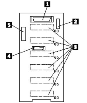
SCSI backplane component locations
The following illustration identifies the SCSI backplane components. Refer to this figure when you set the jumpers on the backplane.
Move the mouse over the index number in the illustration below. Click the index number to locate the description.
| Index | Description |
|---|---|
| 1 | Wide (16-bit) SCSI connector |
| 2 | Option jumper block (J10) |
| 3 | SCSI hot-swap drive connectors (on reverse side of backplane) |
| 4 | Repeater card connector |
| 5 | Power connector |
SCSI backplane option jumpers
The SCSI backplane option jumper block (J10) defines the SCSI IDs for hot-swap drives.
| Pins | Description |
|---|---|
| 1-2 | Reserved. |
| 3-4 | Reserved. |
| 5-6 | Placing a jumper on these two pins enables SCSI IDs 8-13 |
| 7-8 | Reserved. |
| 9-10 | Reserved. |
| 11-12 | Placing a jumper on these two pins reverses the SCSI IDs on the backplane |
NOTE: The default is no jumpers installed on the J10 jumper block.
SCSI IDs for hot-swap hard disk drives| J10 pins 5-6 | J10 pins 11-12 | Bay 1 | Bay 2 | Bay 3 | Bay 4 | Bay 5 | Bay 6 |
|---|---|---|---|---|---|---|---|
| No jumper | No jumper | 0 | 1 | 2 | 3 | 4 | 5 |
| No jumper | Jumper | 5 | 4 | 3 | 2 | 1 | 0 |
| Jumper | No jumper | 13 | 12 | 11 | 10 | 9 | 8 |
NOTES:
- No jumper on pins 5-6 and 11-12 is the default.
- Jumpers on pins 5-6 and 11-12 is not supported.
System board component locations
The following illustration identifies system board component locations. You might need to refer to this figure before you install hardware in the server, or when you record information in the tables in this chapter. You might also need to refer to this figure when you set configuration jumpers on the system board.
Move the mouse over the index number in the illustration below. Click the index number to locate the description.
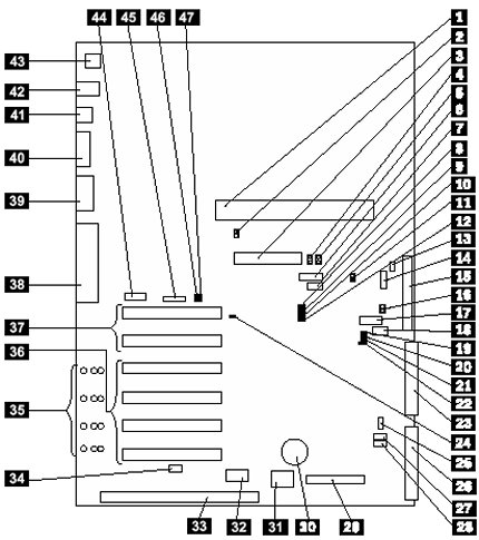
System board jumpers
WARNING: Turn off the server, and disconnect the power cords before moving any jumpers.
| Index | Jumper Name | Description |
|---|---|---|
| 8 | J11 Disable RAID controller | The default position is Enabled (jumper on pins 1 and 2). Move the the jumper to pins 2 and 3 to disable the RAID controller. |
| 9 | J45 Reserved | The default position is a jumper on pins 2 and 3. |
| 10 | J32 Power on control | The default position is normal operation (jumper on pins 1 and 2). Moving the jumper to pins 2 and 3 allows the power supply to be turned on without a control panel or system management processor. |
| 11 | J15 RAID download | The default position is no jumpers on the pins. This jumper block is used when the RAID adapter EEPROM is being updated. |
| 12 | J25 Reserved | The default position is a jumper on pins 1 and 2. |
| 13 | J9 Reserved | The default position is a jumper on pins 1 and 2. |
| 20 | J34 Reserved | The default position is a jumper installed on pins 1 and 2. |
| 21 | J29 Reserved | The default position is a jumper installed on pins 1 and 2. |
| 22 | J26 Reserved | The default is no jumper installed on J26. |
| 24 | J51 Disable Advanced System Management processor | In normal operation, there is no jumper on J51. Installing a jumper on J51 disables the Netfinity Advanced System Management processor. |
| 27 | J24 Power on password override | Changing the position of this jumper bypasses the power-on password check if the jumper has been moved since the server was last powered on. You do not need to move the jumper back to the default position after the password is overridden. Changing the position of this jumper does not affect the administrator password check if an administrator password is set. |
| 28 | J30 Flash ROM page swap | The default position is a jumper installed on pins 2 and 3. Changing the position of this jumper will change which of the two pages of Flash ROM is used when the system is started. |
| 46 | J5 Disable Ethernet controller | The default position is Enabled (jumper on pins 1 and 2). Move the the jumper to pins 2 and 3 to disable the Ethernet controller. |
| 47 | J14 Disable video controller | The default position is Enabled (jumper on pins 1 and 2). Move the the jumper to pins 2 and 3 to disable the video controller. |
NOTE: The numbers in the table correspond to the highlighted numbers on System board component locations illustration above.
Processor board component locations
The following illustration identifies processor board component locations.
Move the mouse over the index number in the illustration below. Click the index number to locate the description.
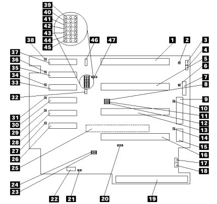
Processor board jumpers
NOTES:
- The numbers in the table correspond to the highlighted numbers on System board component locations illustration above.
- Turn off the server, and disconnect the power cords before moving any jumpers.
- Be sure the microprocessor bus-to-core ratio is set correctly. For example, if you have a 400MHz 2 microprocessor installed and the system
bus speed is 100MHz (the default), be sure thatthe microprocessor core frequency selection switch block is set to a bus-to-core ratio of 4 (400/100).
WARNING: If the microprocessor bus-to-core ratio is incorrect, system board components will overheat and component damage might occur. Be sure that the microprocessor core-frequency selection is properly set.
Processor board jumpers| Index | Jumper name | Description |
|---|---|---|
| 20 | J24 Reserved | The default position is a jumper on pins 1 and 2. |
| 22 | J37 Reserved | The default position is a jumper on pins 1 and 2. |
| 23 | J21 Reserved | The default position is a jumper on pins 2 and 3. |
| 24 | J20 Reserved | The default position is a jumper on pins 1 and 2. |
| 39 - 42 | J31–J28 Microprocessor core frequency selection | For the core/bus fraction 4 (400/100MHz), jumpers are installed on pins 1 and 2 of J28, J30, and J31 and on pins 2 and 3 of J29. For the core/bus fraction 4.5 (450/100MHz), jumpers are installed on pins 1 and 2 of J28 and J31 and on pins 2 and 3 of J29 and J30. For the core/bus fraction 5 (500/100MHz), jumpers are installed on pins 1 and 2 of J30 and J31 and on pins 2 and 3 of J28 and J29. |
| 43 | J27 Reserved | The default position is a jumper on pins 1 and 2. |
| 44 | J25 Reserved | The default position is a jumper on pins 1 and 2. |
| 45 | J26 Reserved | The default position is a jumper on pins 2 and 3. |
| 47 | J34 Reset system | The default position for normal operation is no jumper on J34. Installing a jumper on pins 1 and 2 will force the system into the reset state. Table 15. Microprocessor core frequency selection switch (SW1) settings |
Microprocessor core frequency selection switch (SW1) settings
| Core/Bus ratio | J28 | J29 | J30 | J31 |
|---|---|---|---|---|
| 4 | Pins 1 and 2 | Pins 2 and 3 | Pins 1 and 2 | Pins 1 and 2 |
| 4.5 | Pins 1 and 2 | Pins 2 and 3 | Pins 2 and 3 | Pins 1 and 2 |
| 5 | Pins 2 and 3 | Pins 2 and 3 | Pins 1 and 2 | Pins 1 and 2 |
| 5.5 | Pins 2 and 3 | Pins 2 and 3 | Pins 2 and 3 | Pins 1 and 2 |
NOTE: For jumper settings for other speed microprocessors, refer to the label on the inside top cover of the server.
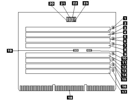
Memory board
The following illustration identifies the Memory board components.
Move the mouse over the index number in the illustration below. Click the index number to locate the description.
Additional information
Document Location
Worldwide
Was this topic helpful?
Document Information
Modified date:
24 January 2019
UID
ibm1MIGR-52663